
My Friends,
EDIT:
Due to confusion of this thread, I want to share this small post, that clears up the confusion:
This thread has not been very successful at pointing out what I meant to point out.
Everyone needs to think in terms of a "Lead up to the main event" so what was said, or explained in earlier threads, is meant for a more board result in the end. Gotta look at the bigger picture.
The point I meant to get to was:
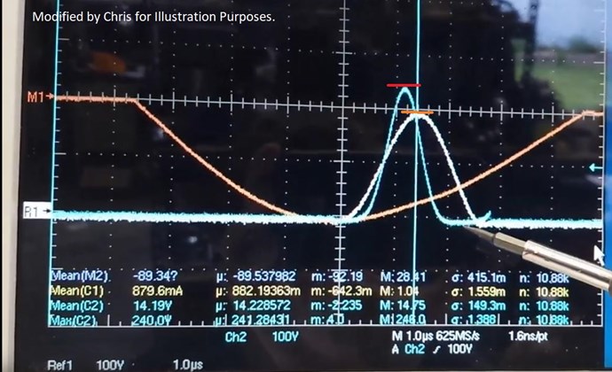
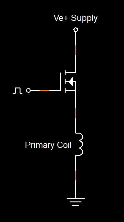
There is a natural delay in Conduction from the Input Coil to POCTwo.
Here is how this works:
- Input Coil is switched on - Changing Current in Time!
- POCOne Conducts and a Voltage builds.
- POCOne's current builds as the Voltage Builds - Changing Current in Time!
- Sufficient Voltage is "Generated" in POCTwo, to now conduct, via the Diode, which was not shown at the time of this thread.
- Voltage keeps building in POCOne and POCTwo, until peak Voltage is reached.
- Your Input Coil is switched off at this point.
- POCOne and POCTwo's voltage decay over time.
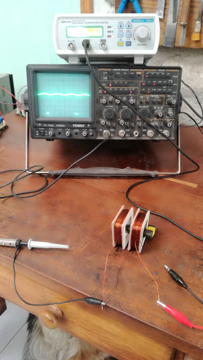
When you do these experiments, you will see, there is a Natural Delay for all of these processes to take place! This is what stops these machines from effectively Running Away on themselves and gives us control over the process, with an external Frequency!
I repeat: There is a natural delay in Conduction from the Input Coil to POCTwo.
End EDIT.
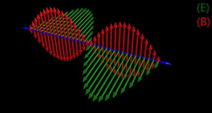
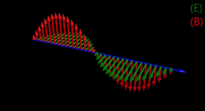
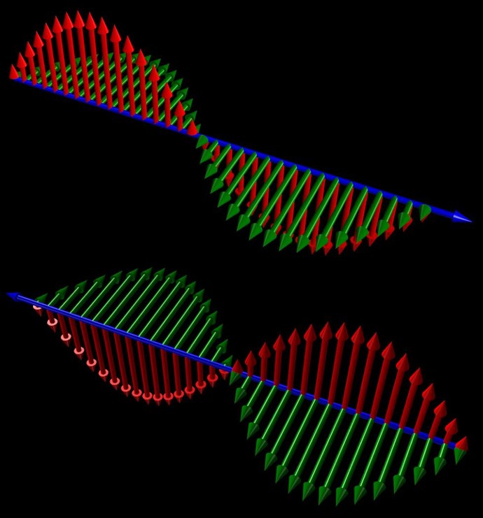
The Effects of Delayed Conduction in Bucking Coils is important. What is Delayed Conduction? What is the point of this?
Delayed Conduction is specifically to get the Voltage on the Terminals of your Partnered Output Coils as high as possible in reason! Its the change in Magnetic Field that Creates Voltage, its the Opposition of Magnetic Fields that Pumps Current!
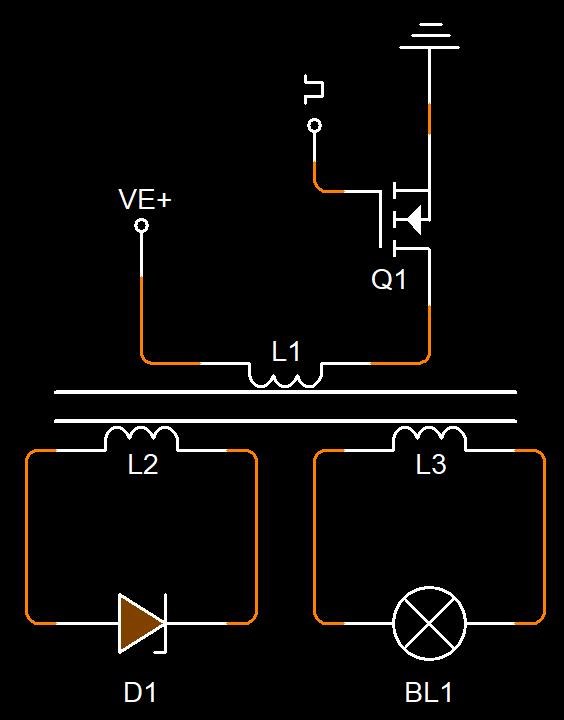
Circuitry can also be employed to delay Conduction on the second Partnered Output Coil.
I gave an example of Delayed Conduction here.
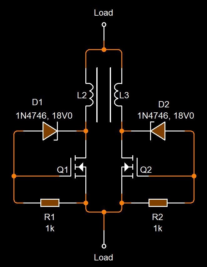
As you can see, the Mosfets will only conduct when the Zener Diodes Conduct, this is rated to 18 Volts.
This means, the ends of the Partnered Output Coils must be at least 18 Volts, before the Coils can power any load!
We have seen this before! This is not new to those that have done the Study!
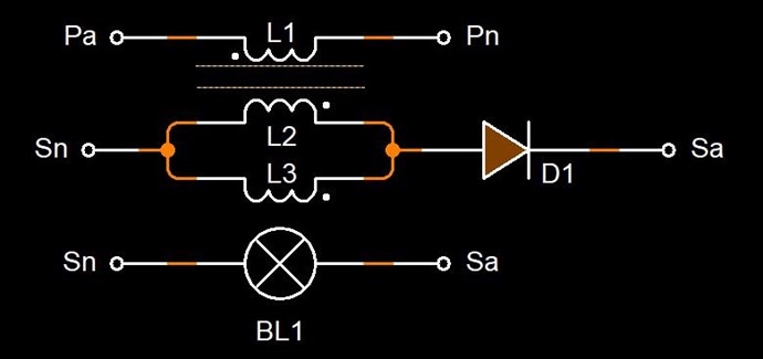
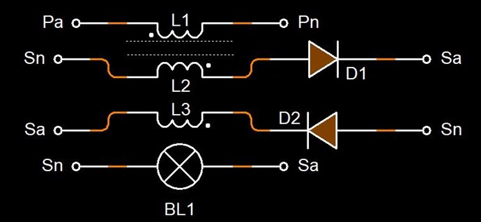
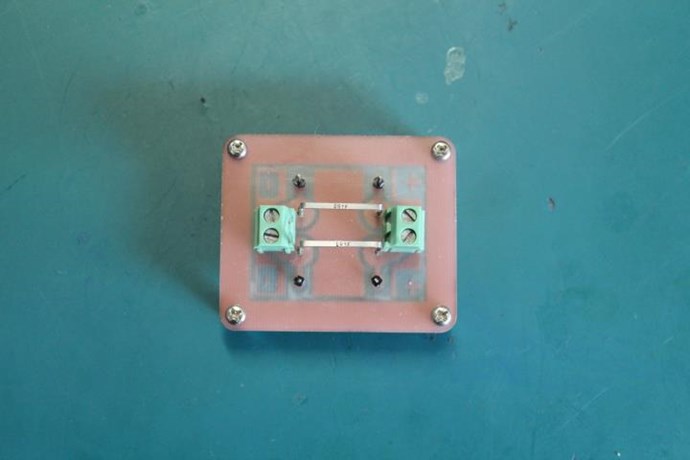
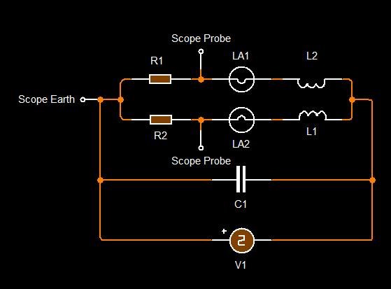
The MEG Demo Circuit
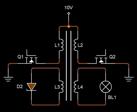
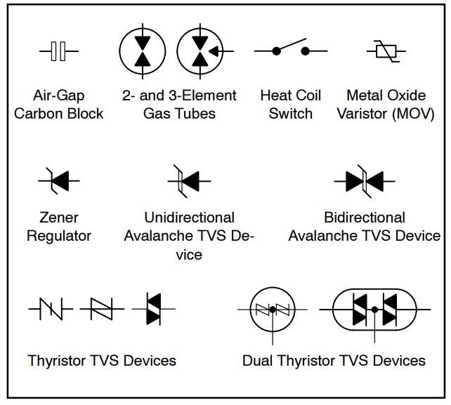
Where D2 represents a Bi-Directional TVS.
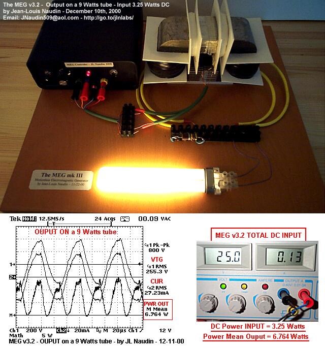
Ref: JLN MEG Replication
Ref: The MEG Team Data.
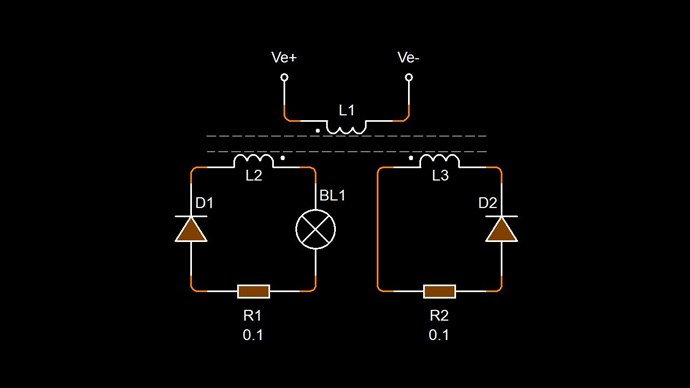
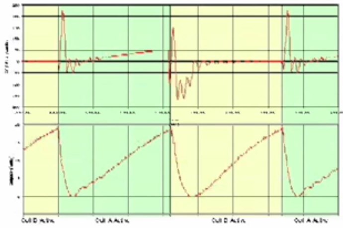
Where the Top Trace represents the Input Channels, and the bottom Trace Magnetic Resonance in the Output Coils, seen as Asymmetrical Regauging.
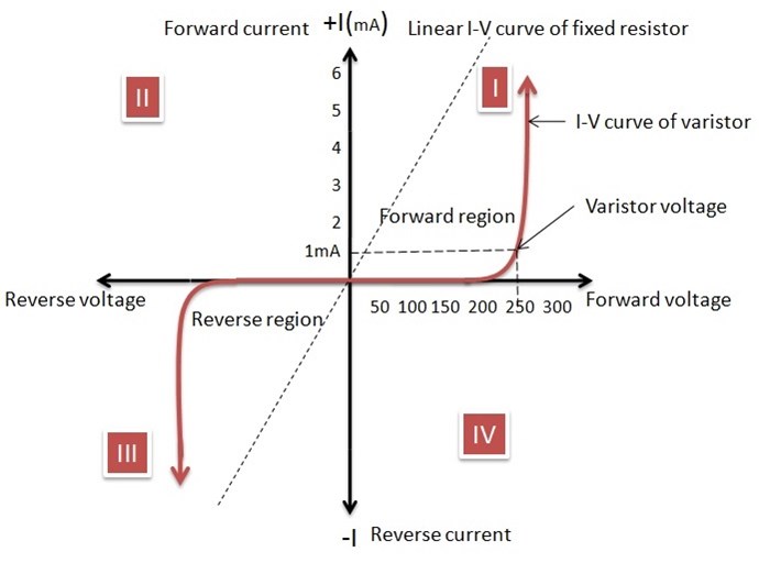
NOTE: JLN used a MOV in his MEG Replication. A MOV has similar Voltage to Current Characteristics!
Ref: JonRB
![]()
Ref: Renesas Datasheet
I want to stress the point of getting the Voltage on the Terminals of your Partnered Output Coils to a maximum without being disturbed. Input Creates a Voltage on your Terminals, then the Input is switched off. Then your Partnered Output Coils Conduct and we Pump Current.
Remember: Some of these Circuits may require an Earth Ground.
Chris


 . I'm not an ee but I do have sufficient electronics skills and I believe that I understand the concepts and theories, as you have presented, quite well. The only problem I have is a lack of time for experimenting. Full time job, family with small children and only 24 hours in a day.